 半導體襯底和外延的區別分析
硅外延層和襯底是半導體制造過程中的兩個重要組成部分。襯底是半導體芯片制造的基礎,主要由單晶硅材料制成。硅外延層是在襯底上加工生長的一層硅材料,其材料特性與襯底相同。二者在成份、結構和性質上都有所不同。
Silicon epitaxial layers and substrates are two important components in the semiconductor manufacturing process. The substrate is the basis for semiconductor chip manufacturing and is mainly made of single crystal silicon material. The silicon epitaxial layer is a layer of silicon material processed and grown on the substrate, and its material properties are the same as the substrate. Both are different in composition, structure and properties.
襯底 Substrate 襯底,作為半導體單晶材料制成的晶圓片,它既可以直接進入晶圓制造流程,用于生產半導體器件;也可通過外延工藝加工,產出外延片。半導體襯底就像一塊“地基”,它支撐著整個半導體結構,確保它不會破裂或損壞。同時,襯底本身也具備一些特殊的電學、光學和機械特性,這些特性對于半導體的性能至關重要。 Substrate, as a wafer made of semiconductor single crystal material, can either directly enter the wafer manufacturing process and be used to produce semiconductor devices; it can also be processed through epitaxial processes to produce epitaxial wafers. The semiconductor substrate is like a "foundation" that supports the entire semiconductor structure and ensures that it will not crack or be damaged. At the same time, the substrate itself also has some special electrical, optical and mechanical properties, which are crucial to the performance of semiconductors.
如果把集成電路比作建筑高樓大廈,那么襯底無疑是那穩固的地基。為確保其支撐作用的發揮,這些材料在晶體結構上必須展現出高度的一致性,如同高純度的單晶硅,其純凈與完美是構建堅固地基的基石。只有當地基堅實可靠,才能確保上方建筑的穩固與完美。簡單來說,沒有合適的襯底,我們就無法構建出穩定且性能良好的半導體器件。 If an integrated circuit is compared to a high-rise building, then the substrate is undoubtedly the solid foundation. In order to ensure their supporting role, these materials must show a high degree of consistency in their crystal structure. Just like high-purity single crystal silicon, its purity and perfection are the cornerstones of building a solid foundation. Only when the foundation is solid and reliable can the stability and perfection of the building above be ensured. Simply put, without the right substrate, we cannot build stable and well-performing semiconductor devices.
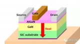
外延 Epitaxy 外延,是指在經過精心切磨拋光的單晶襯底上,精準生長一層全新單晶的過程。這層新單晶既可與襯底材質相同(同質外延),也可不同(異質外延)。由于新生單晶層嚴格遵循襯底晶相延伸生長,因此被稱為外延層,其厚度通常控制在幾微米級別。以硅為例,外延生長即在特定晶向的硅單晶襯底上,形成一層晶向一致、電阻率和厚度各異、晶格結構完整的新晶體。經過外延生長的襯底則被稱為外延片,其核心價值在于外延層,而器件制作正是圍繞這一層展開。 Epitaxy refers to the process of accurately growing a new layer of single crystal on a carefully cut and polished single crystal substrate. This new single crystal can be made of the same material as the substrate (homoepitaxial) or different (heteroepitaxial). Because the new single crystal layer strictly follows the crystalline phase of the substrate and grows, it is called an epitaxial layer, and its thickness is usually controlled at the level of a few microns. Taking silicon as an example, epitaxial growth is to form a layer of new crystals with the same crystal orientation, different resistivities and thicknesses, and a complete lattice structure on a silicon single crystal substrate with a specific crystal orientation. The epitaxially grown substrate is called an epitaxial wafer. Its core value lies in the epitaxial layer, and device production revolves around this layer. 外延片的價值體現在其巧妙的材料組合上。例如,通過在成本較低的硅片上生長一層薄薄的GaN外延,便能以相對低廉的第一代半導體材料為襯底,部分實現昂貴且性能卓越的第三代半導體寬禁帶特性,實現高性價比。然而,異質外延結構也伴隨著一系列挑戰,如晶格失配、溫度系數不一致及熱傳導不良等問題,如同將腳手架搭建在塑料地基上,不同材質在溫度變化時會產生膨脹收縮差異,且硅的導熱性能并不理想。
The value of epitaxial wafers is reflected in their ingenious combination of materials. For example, by growing a thin layer of GaN epitaxy on a lower-cost silicon wafer, it is possible to partially realize the wide bandgap characteristics of expensive and excellent third-generation semiconductors using relatively inexpensive first-generation semiconductor materials. , achieving high cost performance. However, heteroepitaxial structures are also accompanied by a series of challenges, such as lattice mismatch, inconsistent temperature coefficients and poor thermal conductivity. Just like building scaffolding on a plastic foundation, different materials will have differences in expansion and contraction when the temperature changes, and Silicon's thermal conductivity is not ideal.
同質外延,即在襯底上生長與襯底材料相同的外延層,其意義在于進一步提升產品的穩定性和可靠性。盡管材料相同,但通過外延處理,晶圓表面的材料純度和均勻度得以顯著提升。相比機械拋光的拋光片,外延片表面更為平整、潔凈,微缺陷和雜質大幅減少,電阻率更加均勻,對表面顆粒、層錯、位錯等缺陷的控制也更加精確。因此,外延技術不僅優化了產品性能,更確保了產品的穩定與可靠。
Homoepitaxy, that is, growing an epitaxial layer that is the same as the substrate material on the substrate, is meant to further improve the stability and reliability of the product. Although the materials are the same, the material purity and uniformity on the wafer surface are significantly improved through epitaxy processing. Compared with mechanically polished polished wafers, the surface of epitaxial wafers is smoother and cleaner, with significantly reduced micro-defects and impurities, more uniform resistivity, and more precise control of defects such as surface particles, stacking faults, and dislocations. Therefore, epitaxy technology not only optimizes product performance, but also ensures product stability and reliability.

總結 Summary
在現代電子、光電子、微電子和信息技術領域,半導體襯底和外延技術都發揮著不可或缺的作用。它們為制造高性能、高可靠性的半導體器件提供了堅實的基礎。隨著科技的不斷發展,半導體襯底和外延技術也將不斷進步,為未來的半導體產業帶來新的突破和發展。
In the fields of modern electronics, optoelectronics, microelectronics and information technology, semiconductor substrates and epitaxial technologies play an indispensable role. They provide a solid foundation for manufacturing high-performance, high-reliability semiconductor devices. With the continuous development of science and technology, semiconductor substrate and epitaxial technology will also continue to advance, bringing new breakthroughs and developments to the future semiconductor industry.
審核編輯:黃飛
-
集成電路
+關注
關注
5392文章
11622瀏覽量
363177 -
半導體芯片
+關注
關注
60文章
919瀏覽量
70777
原文標題:小科普:半導體襯底和外延有什么區別?
文章出處:【微信號:深圳市賽姆烯金科技有限公司,微信公眾號:深圳市賽姆烯金科技有限公司】歡迎添加關注!文章轉載請注明出處。
發布評論請先 登錄
相關推薦
半導體制造之外延工藝詳解
常見幾種SOI襯底及隔離的介紹
CMOS工藝一般都是用P襯底而不是N襯底?兩者有什么區別啊?
不同襯底風格的GaN之間有什么區別?
《炬豐科技-半導體工藝》GaN 基板的表面處理
半導體晶圓材料的基本框架與半導體產業鏈流程
幾種led襯底的主要特性對比 氮化鎵同質外延的難處
半導體器件為什么要有襯底及外延層之分呢?外延層的存在有何意義?
半導體襯底材料的選擇
半導體襯底和外延有什么區別?
異質外延對襯底的要求是什么?

襯底VS外延:半導體制造中的關鍵角色對比

用于半導體外延片生長的CVD石墨托盤結構


 工商網監
工商網監
評論