 電子發燒友App


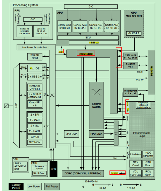
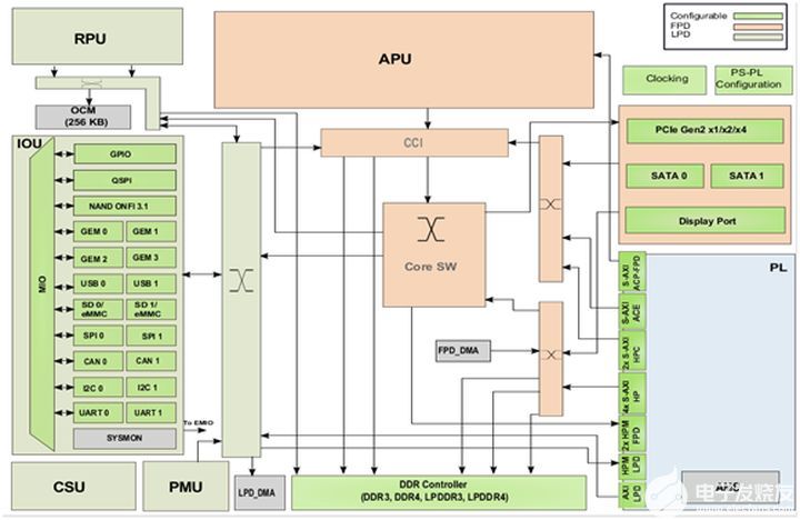
Avnet公司的ZynqUltraScale+ MPSoC系列開發板Ultra96是基于Xilinx® UltraScale™ MPSoC架構.單一器件集成了特性豐富的64位四核或雙核ARM® Cortex™-A53和雙核ARM Cortex-R5處理系統(PS)以及Xilinx可編邏輯(PL)UltraScale架構;此外還集成了片上存儲器,多端口外接存儲器接口,以及豐富的外設連接接口.處理單元的CPU頻率高達1.5GHz,采用ARMv8-A架構,64位或32位工作模式,主要用在工業,IoT (物聯網),嵌入式設計與開發和電子設計.本文介紹了Zynq® UltraScale+™ MPSoC系列主要特性以及開發板Ultra96主要特性,框圖,電路圖,材料清單和PCB設計圖.
The Zynq® UltraScale+™ MPSoC family is based on the Xilinx® UltraScale™ MPSoC architecture. Thisfamily of products integrates a feature-rich 64-bit quad-core or dual-core ARM® Cortex™-A53 anddual-core ARM Cortex-R5 based processing system (PS) and Xilinx programmable logic (PL)UltraScalearchitecture in a single device. Also included are on-chip memory, multiport external memory interfaces,and a rich set of peripheral connectivity interfaces.
Zynq® UltraScale+™ MPSoC系列主要特性:
Processing System (PS)
ARM Cortex-A53 Based Application
Processing Unit (APU)
• Quad-core or dual-core
• CPU frequency: Up to 1.5GHz
• Extendable cache coherency
• ARMv8-A Architecture
o 64-bit or 32-bit operating modes
oTrustZone security
o A64 instruction set in 64-bit mode,A32/T32 instruction set in 32-bit mode
• NEON Advanced SIMD media-processing engine
• Single/double precision Floating Point Unit (FPU)
• CoreSight™ and Embedded Trace Macrocell (ETM)
• Accelerator Coherency Port (ACP)
• AXI Coherency Extension (ACE)
• Power island gating for each processor core
• Timer and Interrupts
o ARM Generic timers support
o Two system level triple-timer counters
o One watchdog timer
o One global system timer
• Caches
o 32KB Level 1, 2-way set-associativeinstruction cache with parity (independent for
each CPU)
o 32KB Level 1, 4-way set-associative datacache with ECC (independent for each CPU)
o 1MB 16-way set-associative Level 2 cachewith ECC (shared between the CPUs)
Dual-core ARM Cortex-R5 BasedReal-Time Processing Unit (RPU)
• CPU frequency: Up to 600MHz
• ARMv7-R Architecture
o A32/T32 instruction set
• Single/double precision Floating Point Unit (FPU)
• CoreSight™ and Embedded Trace Macrocell(ETM)
• Lock-step or independent operation
• Timer and Interrupts:
o One watchdog timer
o Two triple-timer counters
• Caches and Tightly Coupled Memories (TCMs)o 32KB Level 1, 4-way set-associative
instruction and data cache with ECC(independent for each CPU)
o 128KB TCM with ECC (independent for eachCPU) that can be combined to become 256KBin lockstep mode
On-Chip Memory
• 256KB on-chip RAM (OCM) in PS with ECC
• Up to 36Mb on-chip RAM (UltraRAM) with ECC inPL
• Up to 35Mb on-chip RAM (block RAM) with ECCin PL
• Up to 11Mb on-chip RAM (distributed RAM) in PL
ARM Mali-400 Based GPU
• Supports OpenGL ES 1.1 and 2.0
• Supports OpenVG 1.1
• GPU frequency: Up to 667MHz
• Single Geometry Processor, Two Pixel Processors
• Pixel Fill Rate: 2 Mpixels/sec/MHz
• Triangle Rate: 0.11 Mtriangles/sec/MHz
• 64KB L2 Cache
• Power island gating
External Memory Interfaces
• Multi-protocol dynamic memory controller
• 32-bit or 64-bit interfaces to DDR4, DDR3,DDR3L, or LPDDR3 memories, and 32-bit
interface to LPDDR4 memory
• ECC support in 64-bit and 32-bit modes
• Up to 32GB of address space using single or dualrank of 8-, 16-, or 32-bit-wide memories
• Static memory interfaces
o eMMC4.51 Managed NAND flash support
o ONFI3.1 NAND flash with 24-bit ECC
o 1-bit SPI, 2-bit SPI, 4-bit SPI (Quad-SPI), ortwo Quad-SPI (8-bit) serial NOR flash
8-Channel DMA Controller
• Two DMA controllers of 8-channels each
• Memory-to-memory, memory-to-peripheral,peripheral-to-memory, and scatter-gather
transaction support
Serial Transceivers
• Four dedicated PS-GTR receivers andtransmitters supports up to 6.0Gb/s data rates
o Supports SGMII tri-speed Ethernet, PCIExpress® Gen2, Serial-ATA (SATA), USB3.0,
and DisplayPort
Dedicated I/O Peripherals and
Interfaces
• PCI Express — Compliant with PCIe® 2.1 basespecification
o Root complex and End Point configurations
o x1, x2, and x4 at Gen1 or Gen2 rates
• SATA Host
o 1.5, 3.0, and 6.0Gb/s data rates as defined bySATA Specification, revision 3.1
o Supports up to two channels
• DisplayPort Controller
o Up to 5.4Gb/s rate
o Up to two TX lanes (no RX support)
• Four 10/100/1000 tri-speed Ethernet MACperipherals with IEEE Std 802.3 and IEEE Std 1588revision 2.0 support
o Scatter-gather DMA capability
o Recognition of IEEE Std 1588 rev.2 PTP frames
o GMII, RGMII, and SGMII interfaces
o Jumbo frames
• Two USB 3.0/2.0 Device, Host, or OTG peripherals,each supporting up to 12 endpoints
o USB 3.0/2.0 compliant device IP core
o Super-speed, high- speed, full-speed, andlow-speed modes
o Intel XHCI- compliant USB host
• Two full CAN 2.0B-compliant CAN bus interfaces
o CAN 2.0-A and CAN 2.0-B and ISO 118981-1standard compliant
• Two SD/SDIO 2.0/eMMC4.51 compliantcontrollers
• Two full-duplex SPI ports with three peripheralchip selects
• Two high-speed UARTs (up to 1Mb/s)
• Two master and slave I2C interfaces
• Up to 78 flexible multiplexed I/O (MIO) (up tothree banks of 26 I/Os) for peripheral pin
assignment
• Up to 96 EMIOs (up to three banks of 32 I/Os)connected to the PL
Interconnect
• High-bandwidth connectivity within PSand between PS and PL
• ARM AMBA® AXI4-based
• QoS support for latency and bandwidth control
• Cache Coherent Interconnect (CCI)
System Memory Management
• System Memory Management Unit (SMMU)
• Xilinx Memory Protection Unit (XMPU)
Platform Management Unit
• Power gates PS peripherals, power islands, andpower domains
• Clock gates PS peripheral user firmware option
Configuration and Security Unit
• Boots PS and configures PL
• Supports secure and non-secure boot modes
System Monitor in PS
• On-chip voltage and temperature sensing
Programmable Logic (PL)
Configurable Logic Blocks (CLB)
• Look-up tables (LUT)
• Flip-flops
• Cascadable adders
36Kb Block RAM
• True dual-port
• Up to 72 bits wide
• Configurable as dual 18Kb
UltraRAM
• 288Kb dual-port
• 72 bits wide
• Error checking and correction
DSP Blocks
• 27 x 18 signed multiply
• 48-bit adder/accumulator
• 27-bit pre-adder
Programmable I/O Blocks
• Supports LVCMOS, LVDS, and SSTL
• 1.0V to 3.3V I/O
• Programmable I/O delay and SerDes
JTAG Boundary-Scan
• IEEE Std 1149.1 Compatible Test Interface
PCI Express
• Supports Root complex and End Pointconfigurations
• Supports up to Gen4 speeds
• Up to five integrated blocks in select devices
100G Ethernet MAC/PCS
• IEEE Std 802.3 compliant
• CAUI-10 (10x 10.3125Gb/s) or
CAUI-4 (4x 25.78125Gb/s)
• RSFEC (IEEE Std 802.3bj) in CAUI-4 configuration
• Up to four integrated blocks in select devices
Interlaken
• Interlaken spec 1.2 compliant
• 64/67 encoding
• 12 x 12.5Gb/s or 6 x 25Gb/s
• Up to four integrated blocks in select devices
Video Encoder/Decoder (VCU)
• Available in EV devices
• Accessible from either PS or PL
• Simultaneous encode and decode
• H.264 and H.265 support
System Monitor in PL
• On-chip voltage and temperature sensing
• 10-bit 200KSPS ADC with up to 17 external inputs
開發板Ultra96
Ultra96™ is an Arm-based, Xilinx ZynqUltraScale+™ MPSoCdevelopment board based on the Linaro 96Boards specifi cation.
The 96Boards’ specifi cations are open and defi ne a standardboard layout for development platforms that can be used bysoftware application, hardware device, kernel, and other systemsoftware developers. Ultra96 represents a unique position in the96Boards community with a wide range of potential peripheralsand acceleration engines in the programmable logic that is notavailable from other offerings.
Ultra96 boots from the provided Delkin 16 GB microSD card, pre-loadedwith PetaLinux. Engineers have options of connecting to Ultra96 througha Webserver using integrated wireless access point capability or to usethe provided PetaLinux desktop environment which can be viewed on theintegrated Mini DisplayPort video output. Multiple application examples andon-board development options are provided as examples.
Ultra96 provides four user-controllable LEDs. Engineers may also interactwith the board through the 96Boards-compatible low-speed and high-speedexpansion connectors by adding peripheral accessories such as those includedin Seeed Studio’s Grove Starter Kit for 96Boards.
Micron LPDDR4 memory provides 2 GB of RAM in a 512M x 32 configuration.Wireless options include 802.11b/g/n Wi-Fi and Bluetooth 4.2 (provides bothBluetooth Classic and Low Energy (BLE)). UARTs are accessible on a header aswell as through the expansion connector. JTAG is available through a header(external USB-JTAG required). I2C is available through the expansion connector.
Ultra96 provides one upstream (device) and two downstream (host) USB 3.0connections. A USB 2.0 downstream (host) interface is provided on the highspeedexpansion bus. Two Microchip USB3320 USB 2.0 ULPI Transceivers andone Microchip USB5744 4-Port SS/HS USB Controller Hub are specified.
The integrated power supply generates all on-board voltages from an external12V supply (available as an accessory).
開發板Ultra96主要特性:
- Xilinx ZynqUltraScale+ MPSoC ZU3EG A484
- Micron 2 GB (512M x32) LPDDR4 Memory
- Delkin 16 GB microSD card + adapter
- Pre-loaded with PetaLinux environment
- Wi-Fi / Bluetooth
- Mini DisplayPort (MiniDP or mDP)
- 1x USB 3.0 Type Micro-B upstream port
- 2x USB 3.0, 1x USB 2.0 Type A downstream ports
- 40-pin 96Boards Low-speed expansion header
- 60-pin 96Boards High-speed expansion header
- 85mm x 54mm form factor
- Linaro 96Boards Consumer Edition compatible
開發板Ultra96包括:
- Ultra96 development board
- 16 GB pre-loaded microSD card + adapter
- Voucher for SDSoC license from Xilinx
- Quick-start instruction card
開發板Ultra96目標應用:
- Artificial Intelligence
- Machine Learning
- IoT/Cloud connectivity for add-on sensors
- Embedded Computing
- Robotics
- Entry level ZynqUltraScale+ MPSoC
開發環境:
- Training, prototyping and proofof-concept demo platform
- Wireless design and demonstrationsusing Wi-Fi and Bluetooth
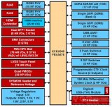
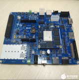
圖1. 開發板Ultra96外形圖
![[原創] Avnet ZynqUltraScale+ MPSoC系列開發方案Ultra96](/uploads/allimg/181211/1R0026092_0.png)
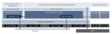
圖2. 開發板Ultra96框圖
![[原創] Avnet ZynqUltraScale+ MPSoC系列開發方案Ultra96](/uploads/allimg/181211/1R1041630_0.png)
圖3. 開發板Ultra96電路圖(1)
![[原創] Avnet ZynqUltraScale+ MPSoC系列開發方案Ultra96](/uploads/allimg/181211/1R2015524_0.png)
圖4. 開發板Ultra96電路圖(2)
![[原創] Avnet ZynqUltraScale+ MPSoC系列開發方案Ultra96](/uploads/allimg/181211/1R301D94_0.png)
圖5. 開發板Ultra96電路圖(3)
![[原創] Avnet ZynqUltraScale+ MPSoC系列開發方案Ultra96](/uploads/allimg/181211/1R401L48_0.png)
圖6. 開發板Ultra96電路圖(4)
![[原創] Avnet ZynqUltraScale+ MPSoC系列開發方案Ultra96](/uploads/allimg/181211/1R5014K2_0.png)
圖7. 開發板Ultra96電路圖(5)
![[原創] Avnet ZynqUltraScale+ MPSoC系列開發方案Ultra96](/uploads/allimg/181211/1R6024622_0.png)
圖8. 開發板Ultra96電路圖(6)
![[原創] Avnet ZynqUltraScale+ MPSoC系列開發方案Ultra96](/uploads/allimg/181211/1RF12225_0.png)
圖9. 開發板Ultra96電路圖(7)
![[原創] Avnet ZynqUltraScale+ MPSoC系列開發方案Ultra96](/uploads/allimg/181211/1RP29335_0.png)
圖10. 開發板Ultra96電路圖(8)
![[原創] Avnet ZynqUltraScale+ MPSoC系列開發方案Ultra96](/uploads/allimg/181211/1RZ13S7_0.png)
圖11. 開發板Ultra96電路圖(9)
![[原創] Avnet ZynqUltraScale+ MPSoC系列開發方案Ultra96](/uploads/allimg/181211/1S0021640_0.png)
圖12. 開發板Ultra96電路圖(10)
![[原創] Avnet ZynqUltraScale+ MPSoC系列開發方案Ultra96](/uploads/allimg/181211/1S1019110_0.png)
圖13. 開發板Ultra96電路圖(11)
![[原創] Avnet ZynqUltraScale+ MPSoC系列開發方案Ultra96](/uploads/allimg/181211/1S2012356_0.png)
圖14. 開發板Ultra96電路圖(12)
![[原創] Avnet ZynqUltraScale+ MPSoC系列開發方案Ultra96](/uploads/allimg/181211/1S301C31_0.png)
圖15. 開發板Ultra96電路圖(13)
![[原創] Avnet ZynqUltraScale+ MPSoC系列開發方案Ultra96](/uploads/allimg/181211/1S4024129_0.png)
圖16. 開發板Ultra96電路圖(14)
![[原創] Avnet ZynqUltraScale+ MPSoC系列開發方案Ultra96](/uploads/allimg/181211/1S5013534_0.png)
圖17. 開發板Ultra96電路圖(15)
![[原創] Avnet ZynqUltraScale+ MPSoC系列開發方案Ultra96](/uploads/allimg/181211/1S6013108_0.png)
圖18. 開發板Ultra96電路圖(16)
![[原創] Avnet ZynqUltraScale+ MPSoC系列開發方案Ultra96](/uploads/allimg/181211/1SF143R_0.png)
圖19. 開發板Ultra96電路圖(17)
![[原創] Avnet ZynqUltraScale+ MPSoC系列開發方案Ultra96](/uploads/allimg/181211/1SP12L3_0.png)
圖20. 開發板Ultra96電路圖(18)
![[原創] Avnet ZynqUltraScale+ MPSoC系列開發方案Ultra96](/uploads/allimg/181211/1SZ155a_0.png)
圖21. 開發板Ultra96電路圖(19)
![[原創] Avnet ZynqUltraScale+ MPSoC系列開發方案Ultra96](/uploads/allimg/181211/1T0011613_0.png)
圖22. 開發板Ultra96電路圖(20)
![[原創] Avnet ZynqUltraScale+ MPSoC系列開發方案Ultra96](/uploads/allimg/181211/1T1015H1_0.png)
圖23. 開發板Ultra96電路圖(21)
![[原創] Avnet ZynqUltraScale+ MPSoC系列開發方案Ultra96](/uploads/allimg/181211/1T2019211_0.png)
圖24. 開發板Ultra96電路圖(22)
![[原創] Avnet ZynqUltraScale+ MPSoC系列開發方案Ultra96](/uploads/allimg/181211/1T3013951_0.png)
圖25. 開發板Ultra96電路圖(23)
![[原創] Avnet ZynqUltraScale+ MPSoC系列開發方案Ultra96](/uploads/allimg/181211/1T402MH_0.png)
圖26. 開發板Ultra96電路圖(24)
![[原創] Avnet ZynqUltraScale+ MPSoC系列開發方案Ultra96](/uploads/allimg/181211/1T502N36_0.png)
圖27. 開發板Ultra96電路圖(25)
![[原創] Avnet ZynqUltraScale+ MPSoC系列開發方案Ultra96](/uploads/allimg/181211/1T60135b_0.png)
圖28. 開發板Ultra96電路圖(26)
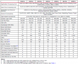
開發板Ultra96材料清單:
![[原創] Avnet ZynqUltraScale+ MPSoC系列開發方案Ultra96](/uploads/allimg/181211/1TF152H_0.png)
![[原創] Avnet ZynqUltraScale+ MPSoC系列開發方案Ultra96](/uploads/allimg/181211/1TP16243_0.png)
![[原創] Avnet ZynqUltraScale+ MPSoC系列開發方案Ultra96](/uploads/allimg/181211/1TZ23R7_0.png)
圖29. 開發板Ultra96 PCB設計圖(1)
圖30. 開發板Ultra96 PCB設計圖(2)
![[原創] Avnet ZynqUltraScale+ MPSoC系列開發方案Ultra96](/uploads/allimg/181211/1U201FA_0.png)
圖31. 開發板Ultra96 PCB設計圖(3)
![[原創] Avnet ZynqUltraScale+ MPSoC系列開發方案Ultra96](/uploads/allimg/181211/1U302E41_0.png)
圖32. 開發板Ultra96 PCB設計圖(4)
圖33. 開發板Ultra96 PCB設計圖(5)
圖34. 開發板Ultra96 PCB設計圖(6)
![[原創] Avnet ZynqUltraScale+ MPSoC系列開發方案Ultra96](/uploads/allimg/181211/1U601L47_0.png)
圖35. 開發板Ultra96 PCB設計圖(7)
圖36. 開發板Ultra96 PCB設計圖(8)
圖37. 開發板Ultra96 PCB設計圖(9)
圖38. 開發板Ultra96 PCB設計圖(10)
![[原創] Avnet ZynqUltraScale+ MPSoC系列開發方案Ultra96](/uploads/allimg/181211/200002HM_0.png)
圖39. 開發板Ultra96 PCB設計圖(11)
![[原創] Avnet ZynqUltraScale+ MPSoC系列開發方案Ultra96](/uploads/allimg/181211/2001019419_0.png)
圖40. 開發板Ultra96 PCB設計圖(12)
![[原創] Avnet ZynqUltraScale+ MPSoC系列開發方案Ultra96](/uploads/allimg/181211/2002013521_0.png)
圖41. 開發板Ultra96 PCB設計圖(13)
![[原創] Avnet ZynqUltraScale+ MPSoC系列開發方案Ultra96](/uploads/allimg/181211/200302O64_0.png)
圖42. 開發板Ultra96 PCB設計圖(14)
![[原創] Avnet ZynqUltraScale+ MPSoC系列開發方案Ultra96](/uploads/allimg/181211/2004025534_0.png)
圖43. 開發板Ultra96 PCB設計圖(15)
![[原創] Avnet ZynqUltraScale+ MPSoC系列開發方案Ultra96](/uploads/allimg/181211/20050324Q_0.png)
圖44. 開發板Ultra96 PCB設計圖(16)
![[原創] Avnet ZynqUltraScale+ MPSoC系列開發方案Ultra96](/uploads/allimg/181211/2006015932_0.png)
圖45. 開發板Ultra96 PCB設計圖(17)
Ultra96 ZynqUltraScale+ ZU3EG Development Board
Ultra96™ is an Arm-based, Xilinx ZynqUltraScale+™ MPSoC development board based on the Linaro 96Boards specifi cation. The 96Boards’specifications are open and define a standard board layout for development platforms that can be used by software application, hardware device, kernel, and other system software developers. Ultra96 represents a unique position in the 96Boards community with a wide range of potential peripherals and acceleration engines in the programmable logic that is not available from other offerings.
Xilinx ZynqUltraScale+ MPSoC ZU3EG A484
Micron 2 GB (512M x32) LPDDR4 Memory
Delkin 16 GB microSD card + adapter
Wi-Fi / Bluetooth
Mini DisplayPort (MiniDP or mDP)
1x USB 3.0 Type Micro-B upstream port
2x USB 3.0, 1x USB 2.0 Type A downstream ports
40-pin 96Boards Low-speed expansion header
60-pin 96Boards High-speed expansion header
85mm x 54mm form factor
Linaro 96Boards Consumer Edition compatible
詳情請見:
https://www.xilinx.com/support/documentation/data_sheets/ds891-zynq-ultrascale-plus-overview.pdf
和
以及https://www.avnet.com/opasdata/d120001/medias/docus/187/AES-ULTRA96-G_2018-03-19.pdf
和https://www.avnet.com/opasdata/d120001/medias/docus/187/AES-ULTRA96-G%20BOM%20REV%201%20180315.pdf
與https://www.avnet.com/opasdata/d120001/medias/docus/187/AES-ULTRA96-G%20layout%20180315.pdf
以及https://www.avnet.com/opasdata/d120001/medias/docus/187/AES-ULTRA96-G%20assembly%20180315.pdf
ds891-zynq-ultrascale-plus-overview.pdf
2645246.pdf
AES-ULTRA96-G_2018-03-19.pdf
AES-ULTRA96-G BOM REV 1 180315.pdf
AES-ULTRA96-G layout 180315.pdf
AES-ULTRA96-G assembly 180315.pdf


 工商網監
工商網監
評論